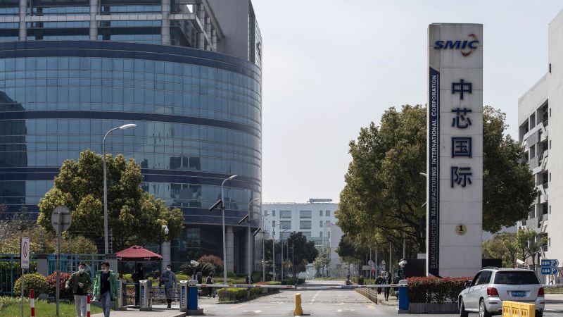
China’s top chipmaker may be in hot water as US lawmakers call for further sanctions after Huawei ‘breakthrough’::Shares in SMIC, China’s largest contract chipmaker, plunged on Thursday, after two US congressmen called on the White House to further restrict export sales to the company.


The chip design is top notch. The manufacturing is 3 generations behind. Its manufactured in 7nm. Current state of the art is 3nm. So more like 3–4 years and not 5, but still behind.
We can’t say anything for certain though, since besides the manufacturing width, yields are important too. If they manage 7nm in a high yield its a completely different story than 7nm with a low yield. In a capitalist system no one would go 7nm with a low yield, but in Chinas system economical viability isn’t a priority.
The real thing that matters is if they reach “good enough”. 7nm/5nm/3nm is a useful technical milestone, and a measure of the quality of their tooling, but at the end of the day, the question is if they can make parts that fulfills a real product need without foreign dependencies.
Size is not everything-- don’t forget when Intel stumbled on 10nm repeatedly, yet they were still printing money with 14nm+++++ because the process was “good enough” to deliver a chip people wanted.
I also have to wonder if the music is going to slow down for some of the IC industry soon. Yeah, we can feed every transistor that can be fabbed into AI/ML, but flagship smartphones are getting both expensive and ridiculous. Are enough people buying a $1500 phone, whose main feature is that it folds into an origami crane, that it can drive new process nodes? Or will a mature 7nm design provide enough performance and battery life for 90% of customers? What’s the current killer app for more than a $200 phone? Maybe the camera, but image sensors have completely different manufacturing constraints.
I am not sure if it is that simple. Their process is using DUV and I assume a ASML lithograpy machine they got from somewhere. The next big step and what the current leading edge uses is EUV, so a different technique.
Unless they get their hands on one of those machines, which I assume will be prevented at all costs through sanctions, they’d have to reengineer that themselves. Something they havent done even for this 7nm lithograpy machine. EUV was decades in the making with an insane amount of research spending. Even with maybe not having to start from scratch this will be a tough nut to crack.
Unless they solve this problem they might push DUV a bit further, but then hit a brick wall. So I am not sure is your estimate how far they are behind is accurate in this sense.
That said, as someone else posted. 7nm is already plenty good for a lot of stuff.